Services
In addition to Xfold bioimaging and diagnostic products, We provide designing, developing and scalable manufacturing services for photonics technology. We have experience and fabrication facilities to both prototype and larger volume manufacturing of micro and nano structures for various applications.
Founded in 2018 , From Aalto University. The team consists of physicists, biologists, biomedical imaging scientists, and business strategists.
Fabrication facilities
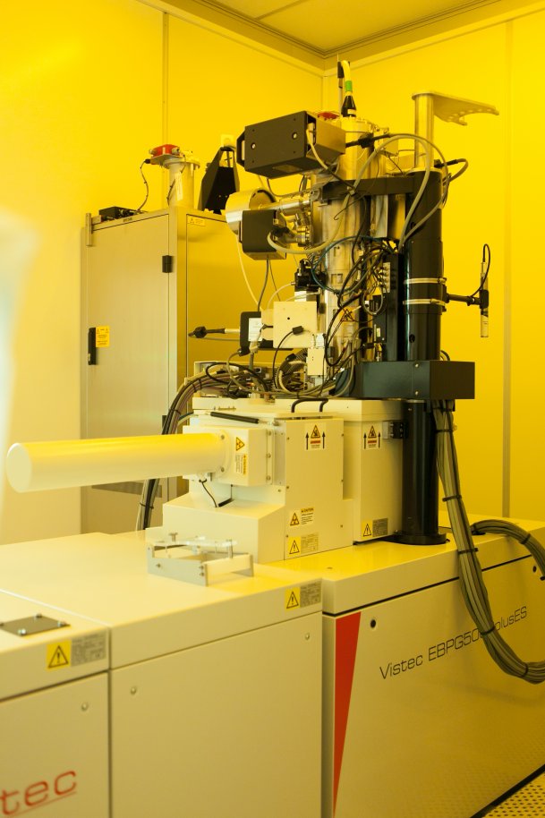
EBL
Resolution: 7.6 nm on 40 nm thick HSQ, 2″, 4″, and 6″ wafers and small pieces down to 5 x 5 mm.
Etching
Reactive Ion Etching (RIE) system with F-based chemistry. Process gases are SF6, CF4, O2, Ar and CHF3.
Substrate size: optimized for 100 mm and Nonuniformity over 100 mm < 2 %
ALD
ALD equipments are designed to the oxide and nitride film deposition. ALDs are mainly used to grow TiO2, ZnO, and Al2O3
Evaporation
Electron beam evaporator used for high resolution nanofabrication with a special focus on depositing metal films -Al, Ti, Ag, Cu, Au, Ge, Cr, Ni
Analysis facilities
AFM and SEM
Bruker Dimension icon
SmartSEM® V05.06
Reflectance/Transmittance measurement
Custom-built reflectance/Transmittance setup with 380 – 950 nm range
Measurement spot size 100 μm – 2 cm
Ellipsometry
Laser wavelength 632.8 nm, Incidence angle range 35- 73deg, Substrate Size: Up to 145 mm
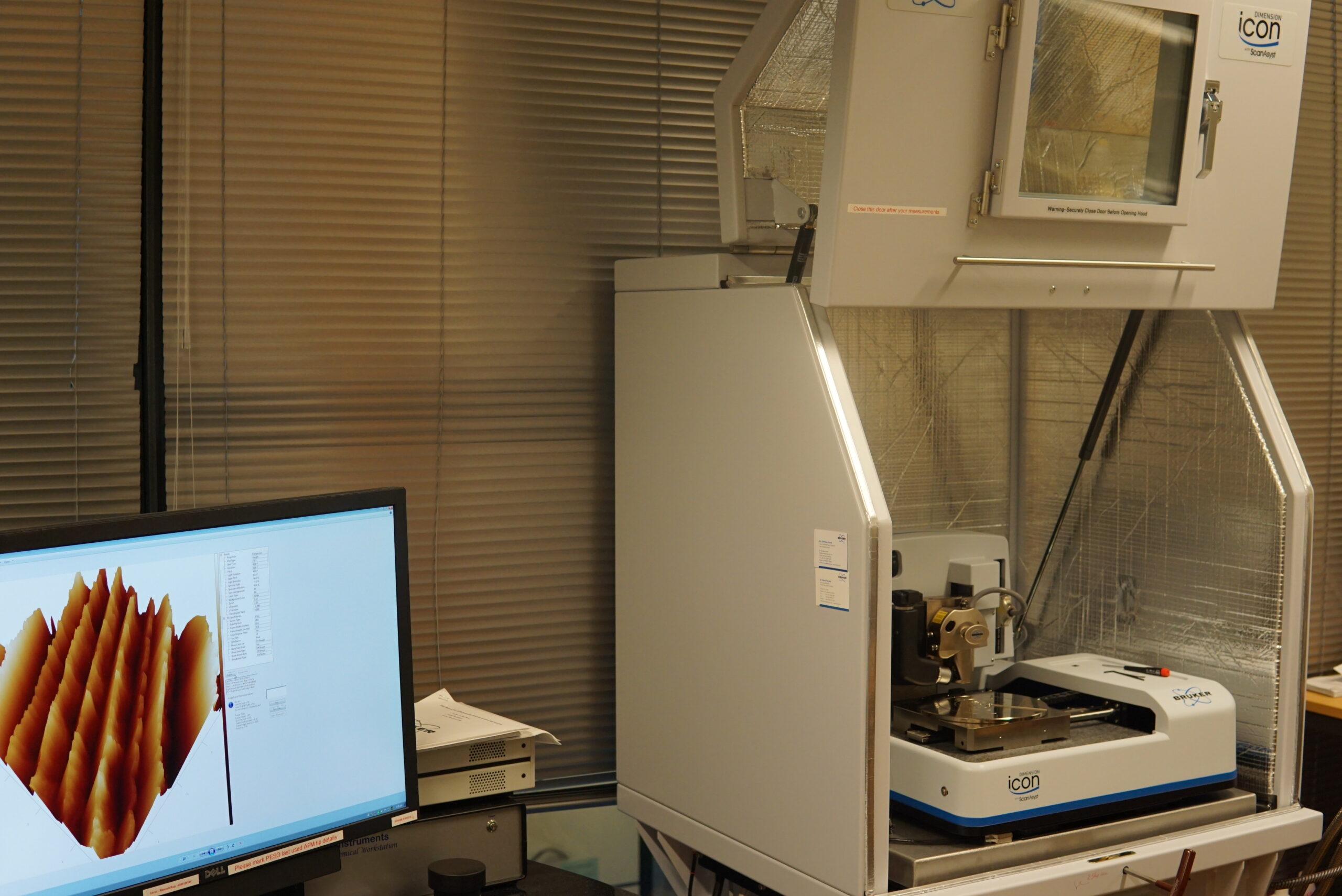
Examples – AFM images of Pillar, hole and grating nanostructures


